

1.6 Nanometer Process: A New Era in Processor Evolution
The race to reduce the process size continues, and leaders in the semiconductor industry are ready to offer incredible innovations. While it seemed not long ago that 5-nm and 3-nm processors were the pinnacle of development, TSMC has already announced the imminent mass production of chips using the 1.6-nanometer process. This is a colossal leap forward, made possible by new architectural solutions and transistor improvements.

From 3000 Nanometers to 1.6: A History of Technological Breakthroughs
To understand the scale of progress, it's worth remembering that the first TSMC chips were produced with a 3-micrometer (3000-nanometer) process. Over several decades, the industry has pushed the boundaries of possibility, densifying transistors and increasing their performance.
Today, the transition to the 1.6-nm process is possible thanks to revolutionary changes in transistor structure and power delivery technology.
Similar developments are underway at Intel, where engineers are developing their own technologies, aiming to regain leadership in processor manufacturing.
The Role of Transistors in Processor Evolution
All modern processors consist of billions of transistors—tiny switches that control electrical current. For decades, transistors have been shrinking, but after the 22-nm process, significant limitations emerged:
- Tunneling effect – electrons began to spontaneously leak through the gate.
- Reduced controllability – decreasing the gate area worsened current control.
To overcome these limitations, engineers transitioned from planar transistors (PlanarFET) to FinFET technology.
The Emergence of FinFET: A Revolution in 3D Transistors
FinFET transistors replaced the flat structure of transistors with three-dimensional fins, allowing:
- Reduced current leakage, as the gate surrounds the channel on three sides.
- Increased control efficiency, reducing power consumption.
- Denser transistor placement, increasing processor power.
However, even this technology eventually reached its limits, as the height and density of the fins cannot grow indefinitely. This is why the industry is now transitioning to GAAFET—a new type of transistor with a ring gate.
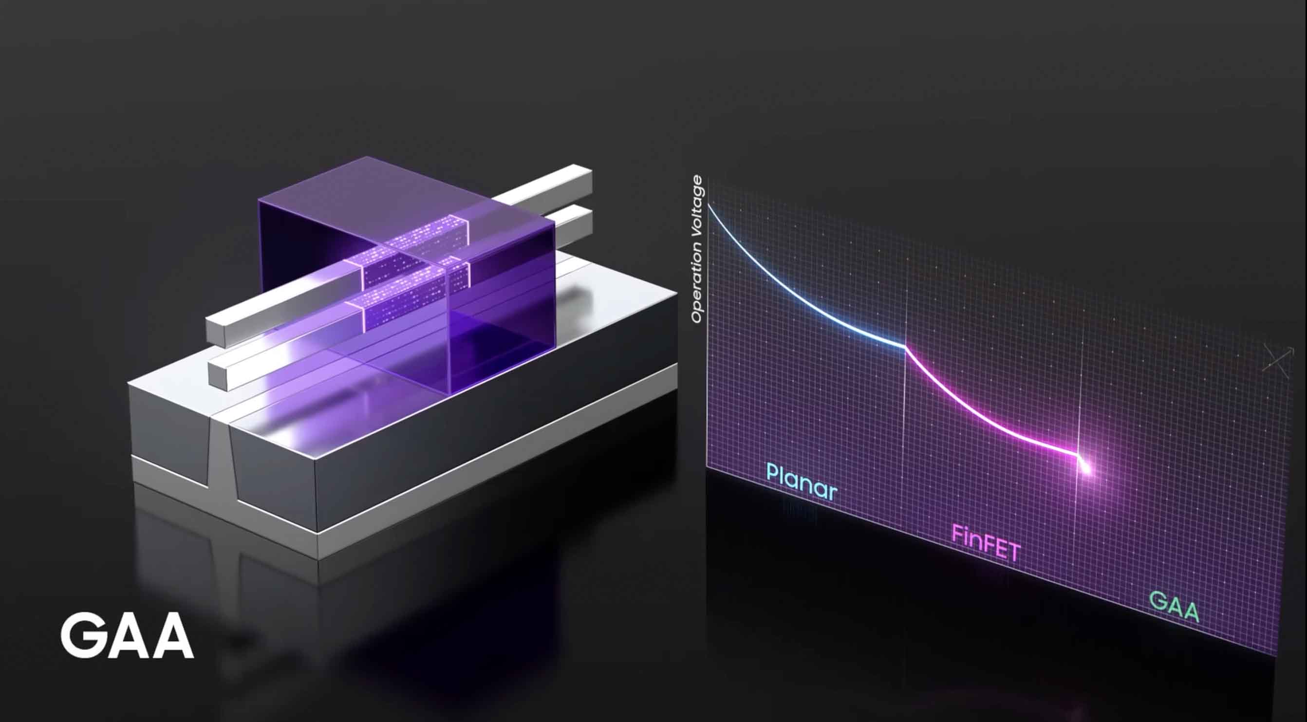
GAAFET: A New Era in Microelectronics
The Gate-All-Around Field-Effect Transistor (GAAFET) technology became the next logical step after FinFET. Instead of elongated fins, engineers created nanosheets that completely surround the channel on all sides.
Thanks to full current control by surrounding the gate on all sides, GAAFETs provide even lower leakage and increased efficiency.
This technology allows overcoming the 3-nanometer barrier and will form the basis of future processors.
Who is Already Developing GAAFET?
Leading semiconductor technology manufacturers are actively investing in GAAFET:
- TSMC announced mass production of GAAFET within the 1.6-nm process.
- Samsung is developing its own version, Multi Bridge Channel FET (MBCFET), using nanosheets instead of nanotubes.
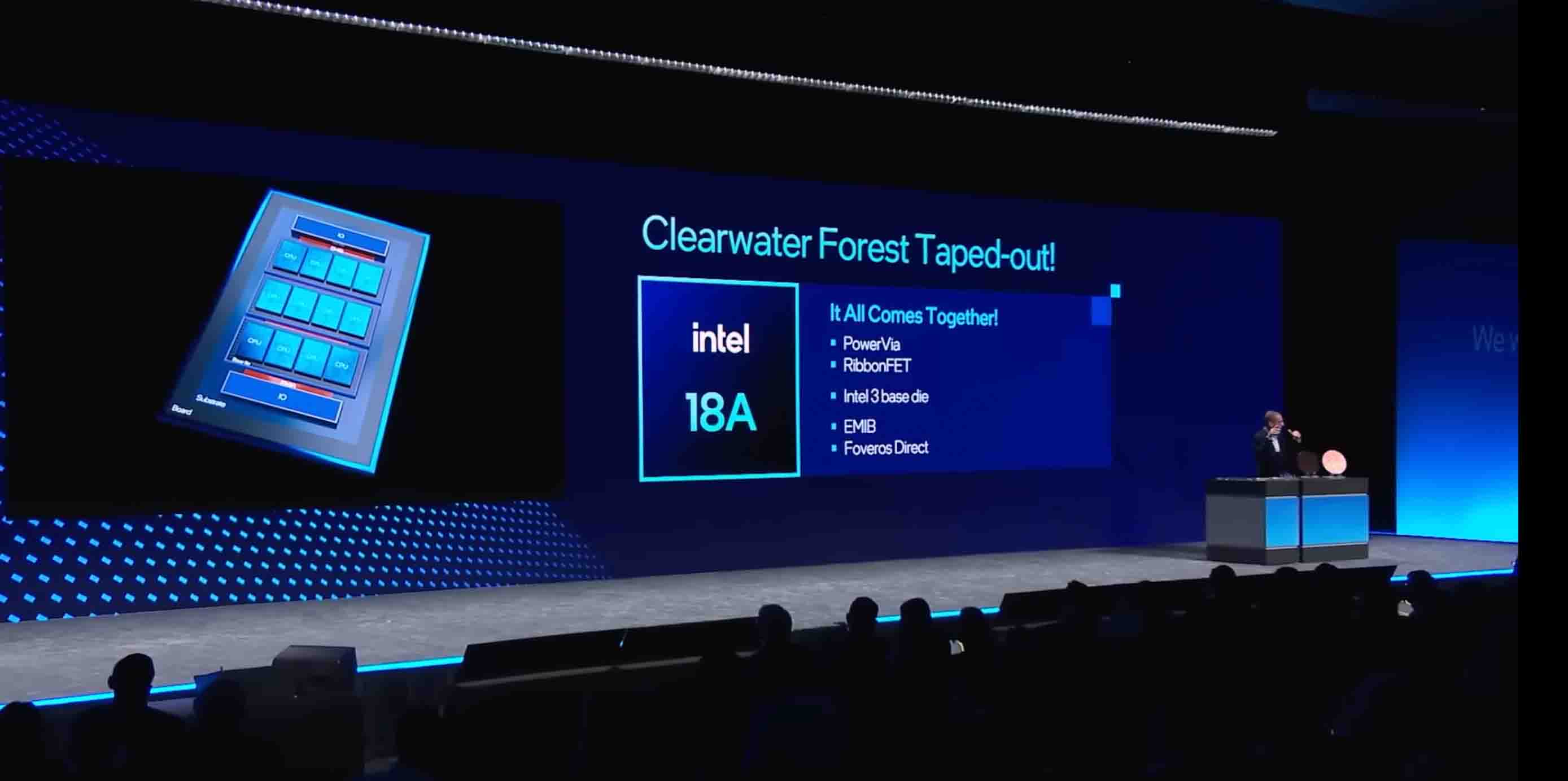
- Intel introduced its version of the technology called RibbonFET, combining ideas from FinFET and GAAFET.
The first processors based on GAAFET are expected to enter mass production by 2025, with commercial chips on the 1.6-nm process expected in 2026.
The development of microelectronics continues at an accelerated pace, and the transition to the 1.6-nm process opens new horizons for computing power. In the coming years, we will see the widespread adoption of GAAFET, followed by possibly even more advanced solutions.
GAAFET Technology: The New Standard in Microelectronics
With the transition to GAAFET (Gate-All-Around Field-Effect Transistor), the semiconductor industry takes a step into a new era. Unlike FinFET, where the gate surrounds the channel on three sides, in GAAFET, the gate surrounds the channel on all four sides. This addresses key issues of previous transistor generations:
- Minimization of current leakage – improved conductivity control reduces parasitic currents.
- Increased energy efficiency – transistors consume less energy at the same performance level.
- Simplified scaling – the ability to further reduce sizes without losing characteristics.
The use of GAAFET allows achieving an improved balance between power, energy consumption, and transistor density, which is critical for modern computing systems.
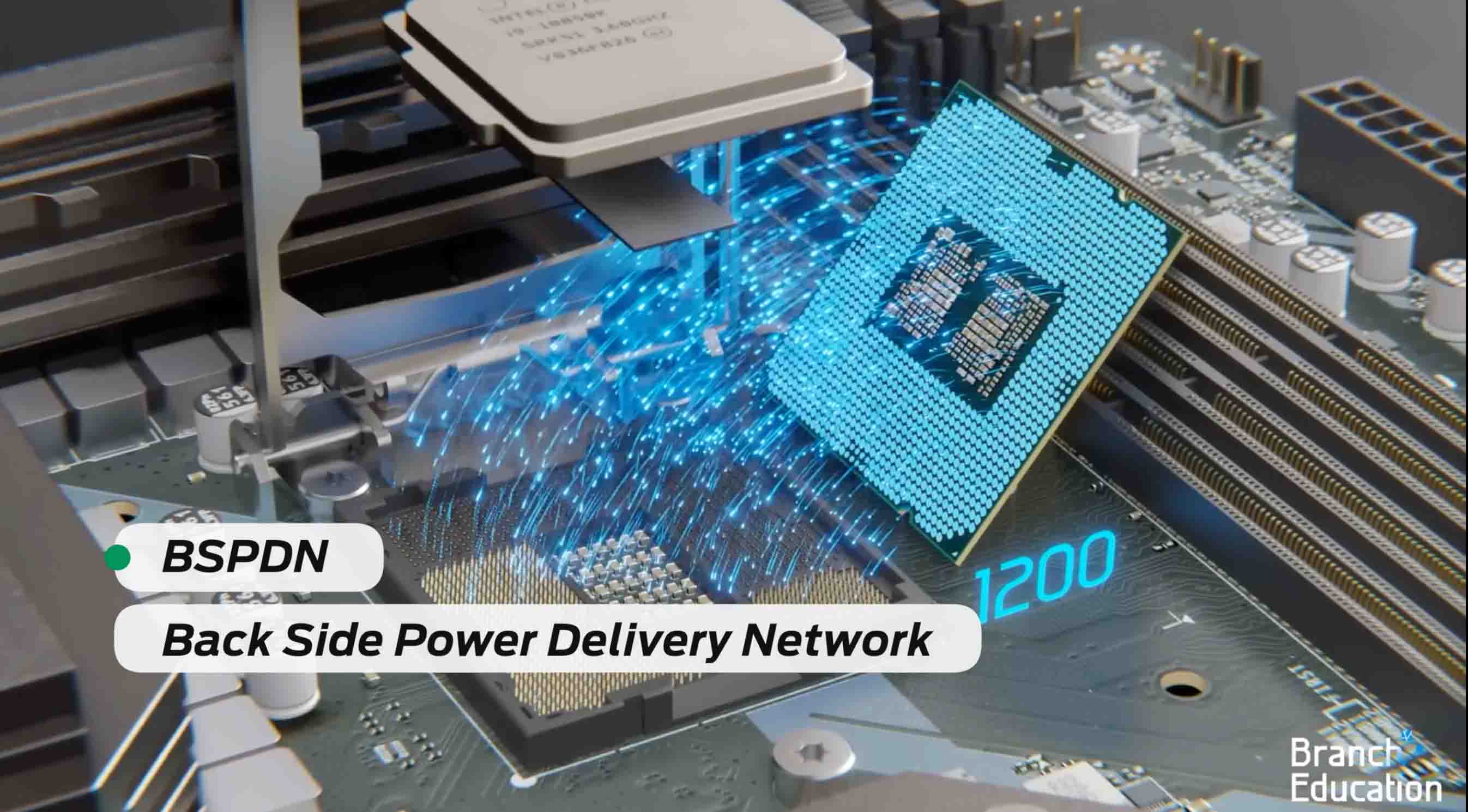
GAAFET and BSPDN: A Dual Revolution in Processors
However, the new 1.6-nm process by TSMC is not just a transition to GAAFET. Another key innovation is the introduction of the Backside Power Delivery Network (BSPDN) technology, or backside power delivery. This means moving all power lines to the backside of the silicon wafer.
Why Move Power to the Backside?
Traditionally, all signal and power lines were placed on one side of the silicon wafer. However, as transistor density increased, this scheme created challenges:
- Complex routing hindered the reduction of transistor sizes.
- Increased power consumption led to higher heat generation.
- Signals lost stability due to high connection densities.
The BSPDN technology allows freeing the front side of the silicon wafer from power lines, simplifying processor design and improving power efficiency.
How Does BSPDN Work?
In traditional processors, power and signal lines are located in one layer, increasing resistance and reducing current stability. BSPDN solves this problem:
- Power lines are moved to the backside of the wafer, reducing resistance and energy losses.
- Signal paths remain on the front side, increasing data transfer speed.
- The number of conductor layers is reduced, simplifying production and lowering lithography costs.
This approach gives processors on the 1.6-nm process significant advantages:
- Reduced power consumption by 15–20%.
- Increased performance by 8–10%.
- Better power management due to reduced resistance.
Who is Developing BSPDN Technology?
Currently, TSMC is the leader in developing BSPDN technology, but other companies are also actively working in this direction:
- Intel has developed its own backside power delivery technology, PowerVia, which will be used in future chips.
- Samsung is also conducting research in this area, adapting BSPDN for its Multi Bridge Channel FET (MBCFET).
Moving power lines to the backside is one of the most revolutionary changes in processor architecture in recent decades.
The Impact of the 1.6-nm Process on the Industry
The introduction of the 1.6-nm process and GAAFET + BSPDN technologies will have a huge impact on various industries:
✔ Artificial Intelligence
Modern AI algorithms require enormous computing power. The new process will allow:
- Creating more energy-efficient AI accelerators.
- Increasing data processing speed without increasing power consumption.
- Optimizing interaction between neural networks and hardware.
✔ Mobile Devices
Thanks to improved energy efficiency and compact transistors, future smartphones will gain:
- Increased battery life.
- More powerful chipsets with less heat generation.
- Support for new image processing technologies and AI functions.
✔ Data Centers and Supercomputers
High transistor density and reduced power consumption make the 1.6-nm process ideal for data centers:
- Reduced cooling costs for server processors.
- Increased computing power per unit area.
- Energy savings for large cloud providers.
When Will the First 1.6-nm Processors Appear?
Although TSMC has already announced the mass production of 1.6-nm processors, the actual market release is expected only by the end of 2026. Reasons for this delay include:
- The high complexity of GAAFET and BSPDN production.
- The need to adapt production capacities.
- Requirements for certification of new semiconductor technologies.
The first to receive 1.6-nm processors will likely be:
- Manufacturers of AI accelerators (NVIDIA, AMD, Google).
- Major cloud solution providers (AWS, Microsoft Azure, Google Cloud).
- Manufacturers of mobile chips (Apple, Qualcomm, MediaTek).
What's Next?
After 1.6-nm processors, the industry is already considering a transition to 1-nm and sub-nanometer technologies. However, further process reduction requires new solutions:
- Using new materials such as graphene and 2D materials.
- Developing quantum transistors to overcome physical limitations.
- Exploring alternatives to silicon electronics, such as optical processors.
The race to reduce the process size continues, and the 1.6-nm process is just the beginning of a new stage in computing technology development.
What Challenges Does the 1.6-nm Process Face?
Despite impressive prospects, the implementation of the 1.6-nm process is associated with several serious technical and economic challenges. Producing such chips requires advanced technologies, and the costs of developing and adapting the new process are colossal.
✔ Complexity of the Lithographic Process
Creating chips with 1.6-nm transistors requires advanced lithography methods. Today, extreme ultraviolet (EUV) lithography is used, but as sizes decrease, the following challenges arise:
- Even higher precision is required when applying semiconductor layers.
- New photoresists are needed that can work with smaller transistor sizes.
- The defect rate on wafers increases, reducing the yield of usable chips.
✔ Increased Production Costs
Each new generation of the process requires significant financial investments:
- Developing 1.6-nm technologies costs billions of dollars.
- Factories need to be re-equipped and new production lines implemented.
- The cost of finished chips significantly increases due to the complexity of their manufacture.
It is expected that the production of 1.6-nm chips will be available only to large corporations working in AI, server technologies, and premium mobile devices.
✔ Heat Dissipation and Power Management
As transistor sizes decrease, their density increases, leading to cooling problems. New architectures, such as BSPDN, help manage overheating, but even they cannot completely eliminate thermal losses.
- Modern processors generate more heat, requiring new cooling systems.
- High transistor density complicates power management.
- Manufacturers are forced to develop new materials for thermal conductivity.
When Will the First Mass Devices with the 1.6-nm Process Appear?
Although TSMC and Intel are actively working on 1.6-nm technologies, mass production will not begin before the end of 2026. It is expected that the first devices with the new process will be:
- Server processors – chips for data centers optimized for cloud computing.
- AI accelerators – specialized chips for machine learning and neural networks.
- Flagship smartphones – mobile processors with improved energy efficiency.
- Gaming GPUs – graphics processors with high performance levels.
It is expected that the first companies to use the 1.6-nm process will be Apple, NVIDIA, AMD, Qualcomm, and other IT industry leaders.
How Will 1.6-nm Processors Affect the Future of Technology?
The transition to 1.6-nm transistors will be an important step in the development of computing technologies. New processors will open up opportunities for:
- More powerful AI algorithms that can operate in real-time.
- Compact and energy-efficient mobile devices with extended battery life.
- Server solutions optimized for heavy loads and data analysis.
- Future 1-nm and sub-nanometer technologies that will replace GAAFET.
However, the main question is how quickly the industry can adapt to such changes. The high cost of development and production may slow down the adoption of the new standard.
Conclusion
The development of processors does not stop, and the transition to the 1.6-nm process will be an important milestone in the history of the semiconductor industry. New technologies, such as GAAFET and BSPDN, will allow achieving:
- Reduced power consumption and increased performance.
- Compact chips with increased transistor density.
- Optimization of computing power for AI and data centers.
However, the implementation of these technologies is associated with enormous technical and economic challenges that must be overcome in the coming years.
The race to reduce the process size continues, and 1.6-nm processors are just the beginning of a new stage in microelectronics development.
The future of computing is becoming even more exciting, and in the coming years, we will see how these technologies change the market for processors, mobile devices, and server solutions.
Stay tuned for updates in the IT world to not miss key achievements in the semiconductor industry!

You may also like our other articles

What Can a Tech Startup Do in 3 Years? What do you think a tech startup can accomplish in three years? Or better yet — what can a robotics-focused IT startup achieve in...
Read the news ⟶
Introduction: A Twist in the Tale of Technology Have you ever wondered why Windows, a system initially designed for mundane office tasks, emerged as the dominant gaming...
Read the news ⟶